Ritesh Agarwal, and A.T. Charlie Johnson (Seed 8)
Monolayer molybdenum disulfide (MoS2) is a 3-atom thick material with a direct band gap, making it of interest for fundamental science as well as applications in optoelectronics and chemical sensing. Our innovation is a scalable method for “seeded growth” of high quality monolayer MoS2 at controlled locations, which is an important advance towards useful applications of the material.
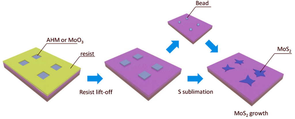
Growth “seeds” of molybdenum-containing material are patterned at known locations with micrometer resolution. Crystalline islands of MoS2 are grown from the seeds by chemical vapor deposition.
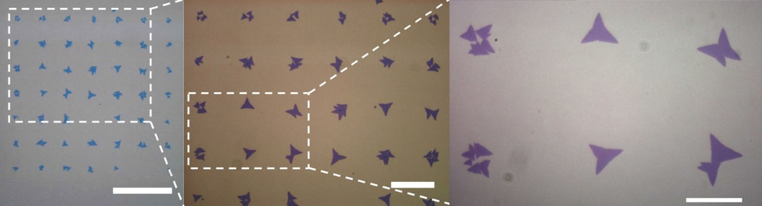
Structural, optical, and electrical measurements show that the growth is high quality monolayer MoS2. With MoS2 islands at known locations, it is straightforward to fabricate MoS2 transistors with minimal chemical contamination for device applications.
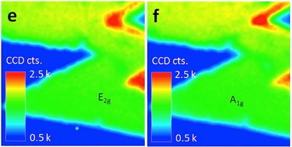
Raman map demonstrates uniformity across monolayer regions.