Ju Li, A.T. Charlie Johnson, Ritesh Agarwal
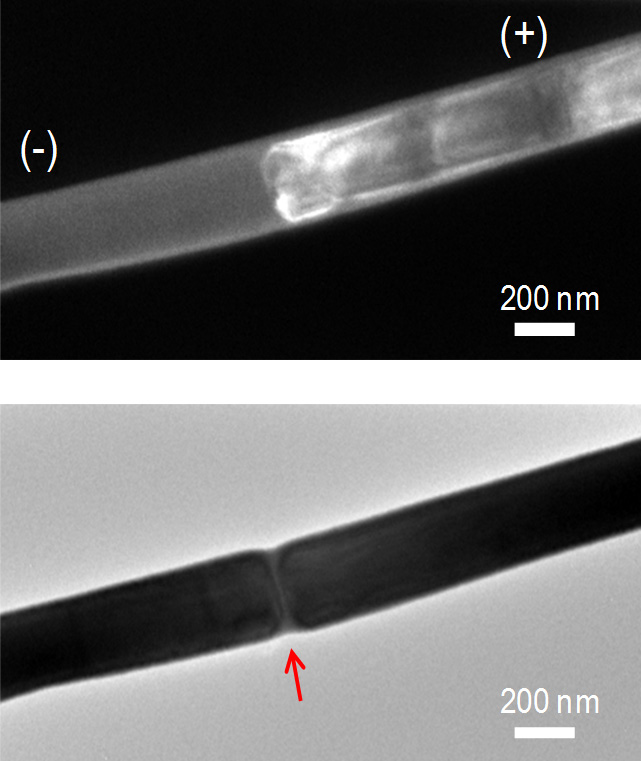
Top: Dark field transmission electron microscopy image of an electrically programmed phase change nanowire. White contrast shows the jammed dislocation cloud which has templated the nanowire along the cross-section. Bottom: Bright field image of the nanowire after amorphization. The red arrow shows the amorphous mark spanning the nanowire cross-section.
Phase-change materials undergo rapid and reversible crystalline-to-amorphous structural transformation and are being used for nonvolatile electronic memory devices. However, the electric-field induced transformation mechanism remains poorly understood and is important to design faster and energy efficient devices. We have studied the effect of electrical pulses on the crystalline-to-amorphous phase change in a single-crystalline nanowire memory device by in situ transmission electron microscopy. Our results show that electrical pulses produce dislocations (defects) in a crystalline material, which become mobile and move in the direction of electrical current. The continuous increase in the density of dislocations moving unidirectionally in the material leads to dislocation jamming, which eventually induces the crystalline-to-amorphous phase change with a sharp interface spanning the entire nanowire cross section. Our work provides evidence of solid-state amophization without forming a liquid melt.
[ Science Magazine Article ] Science, Vol. 336 no. 6088 pp. 1561-1566, 2012